- 您现在的位置:买卖IC网 > Sheet目录1992 > CY28548ZXC (Silicon Laboratories Inc)IC CLK CK505 960M/965M 64TSSOP
CY28548
...................... Document #: 001-08400 Rev ** Page 11 of 30
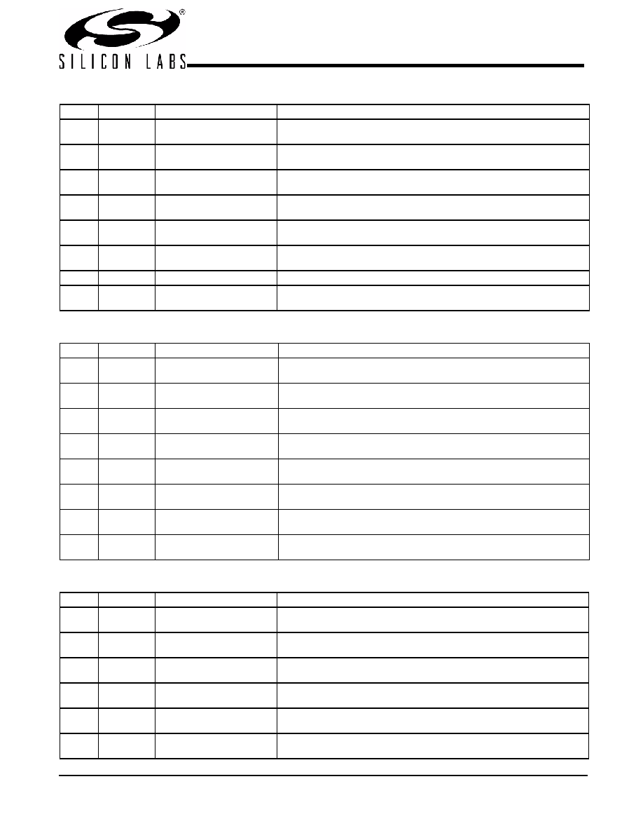
Byte 3: Control Register 3
Bit
@Pup
Name
Description
7
1
SRC[T/C]11
Output enable for SRC11
0 = Output Disabled, 1 = Output Enabled
6
1
SRC[T/C]10
Output enable for SRC10
0 = Output Disabled, 1 = Output Enabled
5
1
SRC[T/C]9
Output enable for SRC9
0 = Output Disabled, 1 = Output Enabled
4
1
SRC[T/C]8/CPU2_ITP
Output enable for SRC8 or CPU2_ITP
0 = Output Disabled, 1 = Output Enabled
3
1
SRC[T/C]7
Output enable for SRC7
0 = Output Disabled, 1 = Output Enabled
2
1
SRC[T/C]6
Output enable for SRC6
0 = Output Disabled, 1 = Output Enabled
1
Reserved
0
1
SRC[T/C]4
Output enable for SRC4
0 = Output Disabled, 1 = Output Enabled
Byte 4: Control Register 4
Bit
@Pup
Name
Description
7
1
SRC[T/C]3
Output enable for SRC3
0 = Output Disabled, 1 = Output Enabled
6
1
SRC[T/C]2/SATA
Output enable for SRC2/SATA
0 = Output Disabled, 1 = Output Enabled
5
1
SRC[T/C]1/LCD_100M[T/C] Output enable for SRC1/LCD_100M
0 = Output Disabled, 1 = Output Enabled
4
1
SRC[T/C]0/DOT96[T/C]
Output enable for SRC0/DOT96
0 = Output Disabled, 1 = Output Enabled
3
1
CPU[T/C]1
Output enable for CPU1
0 = Output Disabled, 1 = Output Enabled
2
1
CPU[T/C]0
Output enable for CPU0
0 = Output Disabled, 1 = Output Enabled
1
PLL1_SS_EN
Enable PLL1s spread modulation,
0 = Spread Disabled, 1 = Spread Enabled
0
1
PLL3_SS_EN
Enable PLL3s spread modulation
0 = Spread Disabled, 1 = Spread Enabled
Byte 5: Control Register 5
Bit
@Pup
Name
Description
7
0
CR#_A_EN
Enable CR#_A (clk req)
0 = Disabled, 1 = Enabled,
6
0
CR#_A_SEL
Set CR#_A
SRC0 or SRC2
0 = CR#_A
SRC0, 1 = CR#_ASRC2
5
0
CR#_B_EN
Enable CR#_B(clk req)
0 = Disabled, 1 = Enabled,
4
0
CR#_B_SEL
Set CR#_B
SRC1 or SRC4
0 = CR#_B
SRC1, 1 = CR#_BSRC4
3
0
CR#_C_EN
Enable CR#_C (clk req)
0 = Disabled, 1 = Enabled
2
0
CR#_C_SEL
Set CR#_C
SRC0 or SRC2
0 = CR#_C
SRC0, 1 = CR#_CSRC2
发布紧急采购,3分钟左右您将得到回复。
相关PDF资料
CY28551LFXC-3T
IC CLOCK INTEL/AMD SIS VIA 56QFN
CY28551LFXC
IC CLOCK INTEL/AMD SIS VIA 64QFN
CY2SSTV855ZXI
IC CLOCK DIFFDRV PLL DDR 28TSSOP
CY2SSTV857ZXI-27
IC CLK DDR266/333BUF1:10 48TSSOP
CY2SSTV857ZXI-32
IC CLK DDR266/333BUF1:10 48TSSOP
CY505YC64DT
IC CLK CK505 BROADWATER 64TSSOP
CYW150OXC
IC CLOCK 440BX AGP 56SSOP
CYW173SXC
IC CLK GEN TAPE DRV 4CH 16SOIC
相关代理商/技术参数
CY28548ZXCT
功能描述:时钟发生器及支持产品 Intel 960/965M Crest line CK505 Intg Vreg RoHS:否 制造商:Silicon Labs 类型:Clock Generators 最大输入频率:14.318 MHz 最大输出频率:166 MHz 输出端数量:16 占空比 - 最大:55 % 工作电源电压:3.3 V 工作电源电流:1 mA 最大工作温度:+ 85 C 安装风格:SMD/SMT 封装 / 箱体:QFN-56
CY28551
制造商:CYPRESS 制造商全称:Cypress Semiconductor 功能描述:Universal Clock Generator for Intel, VIA, and SIS㈢
CY28551-3
制造商:CYPRESS 制造商全称:Cypress Semiconductor 功能描述:Universal Clock Generator for Intel, VIA and SIS㈢
CY28551LFXC
功能描述:时钟发生器及支持产品 Universal System Clk Intel AMD SiS Via RoHS:否 制造商:Silicon Labs 类型:Clock Generators 最大输入频率:14.318 MHz 最大输出频率:166 MHz 输出端数量:16 占空比 - 最大:55 % 工作电源电压:3.3 V 工作电源电流:1 mA 最大工作温度:+ 85 C 安装风格:SMD/SMT 封装 / 箱体:QFN-56
CY28551LFXC-3
功能描述:时钟发生器及支持产品 Universal System Clk Intel AMD SiS Via RoHS:否 制造商:Silicon Labs 类型:Clock Generators 最大输入频率:14.318 MHz 最大输出频率:166 MHz 输出端数量:16 占空比 - 最大:55 % 工作电源电压:3.3 V 工作电源电流:1 mA 最大工作温度:+ 85 C 安装风格:SMD/SMT 封装 / 箱体:QFN-56
CY28551LFXC-3T
功能描述:时钟发生器及支持产品 Universal System Clk Intel AMD SiS Via RoHS:否 制造商:Silicon Labs 类型:Clock Generators 最大输入频率:14.318 MHz 最大输出频率:166 MHz 输出端数量:16 占空比 - 最大:55 % 工作电源电压:3.3 V 工作电源电流:1 mA 最大工作温度:+ 85 C 安装风格:SMD/SMT 封装 / 箱体:QFN-56
CY28551LFXCT
功能描述:时钟发生器及支持产品 Universal System Clk Intel AMD SiS Via RoHS:否 制造商:Silicon Labs 类型:Clock Generators 最大输入频率:14.318 MHz 最大输出频率:166 MHz 输出端数量:16 占空比 - 最大:55 % 工作电源电压:3.3 V 工作电源电流:1 mA 最大工作温度:+ 85 C 安装风格:SMD/SMT 封装 / 箱体:QFN-56
CY2862-000
制造商:TE Connectivity 功能描述:82A0111-4-9-G110